Key Takeaways:
- The second-generation "non-von Neumann" architecture dedicated ASIC chip has completed design and will be produced based on mature domestic semiconductor process technology.
- The chip targets atomic-scale scientific computing, aiming to break through the memory wall and power wall of traditional CPU/GPU, improving long-duration/large-system simulation speed and reducing costs.
- The team developed the first-generation architecture in 2022 and launched the first-generation product in 2023; in 2024, they proposed the second-generation design and advanced technology transfer.
- Hunan Peisen Electronic Technology, in which Hunan University holds equity, and the management team jointly established Guangdong Chipierce, which received strategic investment from Dowstone Technology.
- Foshan's first large-scale Computing Center dedicated to atomic-scale computing has been put into operation, applied to lithium battery, alloy, and nuclear material R&D, serving more than 30 organizations.
Recently, Science and Technology Daily reported on Chipierce’s latest progress in specialized chips for atomic-level scientific computing. According to the report, the “non-von Neumann” architecture specialized ASIC chip (Application Specific Integrated Circuit) independently developed by the team of Professor Liu Jie, co-founder, Chairman and Chief Scientist of Chipierce, has officially completed chip design and is about to enter production based on mature domestic semiconductor processes.
About Science and Technology Daily
Science and Technology Daily is a central mainstream comprehensive daily newspaper founded in 1986 and publicly distributed at home and abroad. It serves as an important public opinion front and main publicity阵地 for the Party and the state in the field of science and technology.
The newspaper focuses on scientific and technological innovation and science popularization, mainly reporting the latest domestic and international S&T developments, national S&T policies, and cutting-edge S&T progress. It is an important window for China’s scientific and technological community to reach society and connect with the world.

Original report
Thank you to Science and Technology Daily for its attention to and coverage of Chipierce. The original report is as follows:
Second-generation “non-von Neumann” architecture specialized ASIC chip about to enter production
On September 9, the reporter learned from Hunan University that the job-related scientific and technological achievement transformation project “non-von Neumann architecture specialized ASIC chip for atomic-level scientific computing,” independently developed by the team of Professor Liu Jie from the university’s School of Integrated Circuits, has officially completed chip design and is about to be produced based on mature domestic semiconductor processes.
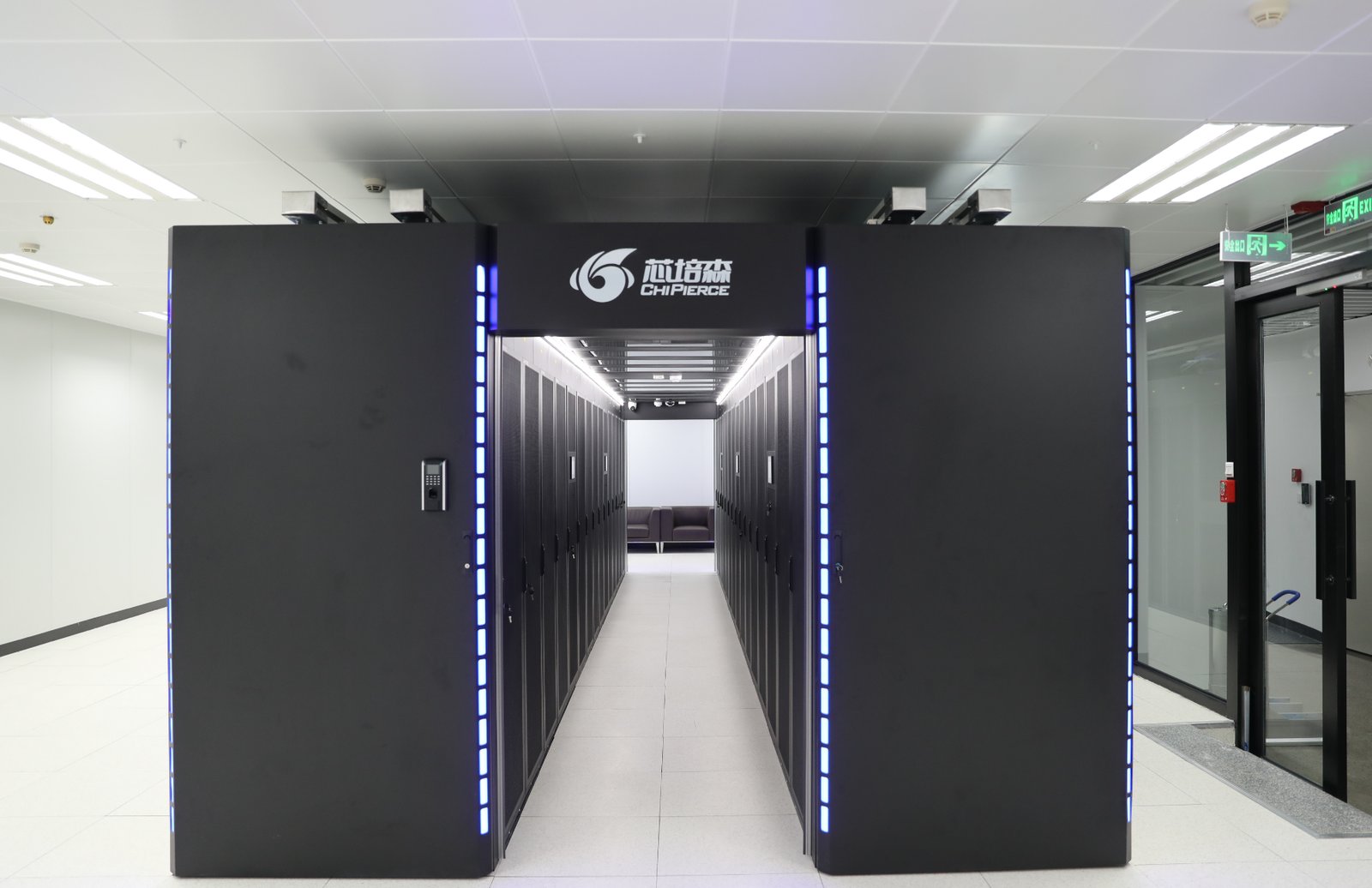
Atomic-level scientific computing, also known as atomic simulation or atomic modeling, calculates the structure, energy, dynamic evolution, and physical properties of material systems at the microscopic level by simulating the motion of electrons and atoms. In atomic-level scientific computing, traditional “von Neumann architecture” CPU/GPU chips have long faced the “memory wall” and “power wall” problems, resulting in slow and costly long-time-scale/large-system atomic simulations that are difficult to implement. To address this challenge, the team independently innovated and developed a “non-von Neumann” specialized chip architecture for atomic simulation, greatly improving computing speed and reducing computing costs compared with CPU/GPU.
In 2022, the team developed the first-generation “non-von Neumann” specialized chip architecture technology and independently developed the first-generation product in 2023. In 2024, the team proposed the design scheme for the second-generation “non-von Neumann” specialized chip architecture and established Hunan Peisen Electronic Technology Co., Ltd., held by Hunan University, for achievement transformation. In the same year, Hunan Peisen Electronic Technology Co., Ltd. jointly established Guangdong Chipierce Technology Co., Ltd. with the management team and received strategic investment from Guangdong Dowstone Technology Co., Ltd. to further carry out achievement transformation.
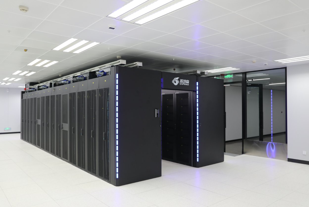
This year, the first large-scale atomic-level computing specialized Computing Center based on the “non-von Neumann” architecture built on the team’s achievements was completed and put into operation in Foshan, Guangdong. It has already been applied to the R&D of multiple key materials, including lithium battery materials, alloy materials, and nuclear materials.
Liu Jie revealed that the successful transformation and further R&D of the project have opened a new path for long-time-scale/large-system materials science computing, breaking through the limitations of traditional CPU/GPU architectures in simulation time scale, system size, and computational energy efficiency. It is expected to help achieve a leap in materials science computing from “nanosecond-level, tens-of-millions-of-atoms-level” to “microsecond-level, hundreds-of-millions-of-atoms-level,” promote the transformation of materials R&D from experiment-driven to computation-driven, and provide a new research tool and technical support for materials innovation in fields such as new energy, semiconductors, and high-end manufacturing.
Up to now, the computing servers developed based on this project have demonstrated excellent performance in computing speed, power consumption, and large-system support, and have been successfully applied by more than 30 enterprises, universities, and research institutes at home and abroad.
Original link:
https://app.kjrb.com.cn/app/template/displayTemplate/news/newsDetail/137/577968.html?isShare=true&xyt=1789103647192